EXEC : instructions per nominal CPU cycle IPC : instructions per CPU cycle FREQ : relation to nominal CPU frequency='unhalted clock ticks'/'invariant timer ticks' (includes Intel Turbo Boost) AFREQ : relation to nominal CPU frequency while in active state (not in power-saving C state)='unhalted clock ticks'/'invariant timer ticks while in C0-state' (includes Intel Turbo Boost) L3MISS: L3 (read) cache misses L3MPKI: L3 misses per kilo instructions L3HIT : L3 (read) cache hit ratio (0.00-1.00) L2DMISS:L2 data cache misses L2DHIT :L2 data cache hit ratio (0.00-1.00) L2DMPKI:number of L2 data cache misses per kilo instruction L2IMISS:L2 instruction cache misses L2IHIT :L2 instructoon cache hit ratio (0.00-1.00) L2IMPKI:number of L2 instruction cache misses per kilo instruction L2MPKI :number of both L2 instruction and data cache misses per kilo instruction
--------------------------------------------------------------------------------------------------------------- TOTAL * 1.29 1.20 1.08 1.00 12 M 0.73 0.04 10 M 0.87 0.03 0.07 19 M 0.00 0.55 N/A
Instructions retired: 336 G ; Active cycles: 281 G ; Time (TSC): 2082 Mticks ; C0 (active,non-halted) core residency: 107.90 %
PHYSICAL CORE IPC : 2.39 => corresponds to 34.14 % utilization for cores in active state Instructions per nominal CPU cycle: 2.58 => corresponds to 36.84 % core utilization over time interval ---------------------------------------------------------------------------------------------------------------
EXEC : instructions per nominal CPU cycle IPC : instructions per CPU cycle FREQ : relation to nominal CPU frequency='unhalted clock ticks'/'invariant timer ticks' (includes Intel Turbo Boost) AFREQ : relation to nominal CPU frequency while in active state (not in power-saving C state)='unhalted clock ticks'/'invariant timer ticks while in C0-state' (includes Intel Turbo Boost) L3MISS: L3 (read) cache misses L3MPKI: L3 misses per kilo instructions L3HIT : L3 (read) cache hit ratio (0.00-1.00) L2DMISS:L2 data cache misses L2DHIT :L2 data cache hit ratio (0.00-1.00) L2DMPKI:number of L2 data cache misses per kilo instruction L2IMISS:L2 instruction cache misses L2IHIT :L2 instructoon cache hit ratio (0.00-1.00) L2IMPKI:number of L2 instruction cache misses per kilo instruction L2MPKI :number of both L2 instruction and data cache misses per kilo instruction
0 0 1.34 1.26 1.06 1.00 8901 K 0.72 3.15 15 M 0.68 5.43 8.58 71 M 4.00 0.60 N/A 1 0 1.42 1.33 1.06 1.00 8491 K 0.73 2.83 14 M 0.68 4.67 7.50 71 M 4.00 0.60 N/A 2 0 1.41 1.33 1.06 1.00 8206 K 0.74 2.75 12 M 0.72 4.25 7.00 71 M 4.00 0.60 N/A 3 0 1.46 1.38 1.06 1.00 7464 K 0.75 2.40 11 M 0.68 3.81 6.21 71 M 4.00 0.60 N/A 4 0 1.31 1.24 1.06 1.00 9118 K 0.71 3.28 15 M 0.69 5.61 8.88 70 M 4.00 0.61 N/A 5 0 1.41 1.33 1.06 1.00 8700 K 0.74 2.92 13 M 0.69 4.66 7.57 70 M 4.00 0.61 N/A 6 0 1.41 1.33 1.06 1.00 8094 K 0.74 2.79 12 M 0.70 4.40 7.18 70 M 4.00 0.61 N/A 7 0 1.43 1.35 1.06 1.00 7873 K 0.74 2.68 12 M 0.71 4.13 6.81 70 M 4.00 0.61 N/A 8 0 1.44 1.36 1.06 1.00 8544 K 0.73 2.79 14 M 0.67 4.87 7.66 20 M 1.00 0.61 N/A 9 0 1.24 1.16 1.06 1.00 524 K 0.51 0.21 86 K 0.94 0.03 0.24 20 M 1.00 0.61 N/A 10 0 1.26 1.18 1.07 1.00 379 K 0.50 0.15 60 K 0.95 0.02 0.17 20 M 1.00 0.61 N/A 11 0 1.24 1.16 1.07 1.00 533 K 0.50 0.20 96 K 0.94 0.04 0.24 20 M 1.00 0.61 N/A 12 0 1.22 1.14 1.07 1.00 1180 K 0.34 0.47 98 K 0.94 0.04 0.51 3872 K 0.12 0.46 N/A 13 0 1.24 1.16 1.07 1.00 409 K 0.49 0.16 64 K 0.94 0.03 0.19 3872 K 0.12 0.46 N/A --------------------------------------------------------------------------------------------------------------- SKT 0 1.18 1.11 1.06 1.00 113 M 0.67 0.73 139 M 0.71 0.89 1.62 186 M 1.12 0.59 N/A SKT 1 1.23 1.14 1.08 1.00 33 M 0.53 0.21 11 M 0.89 0.07 0.28 38 M 0.12 0.45 N/A --------------------------------------------------------------------------------------------------------------- TOTAL * 1.21 1.13 1.07 1.00 147 M 0.65 0.46 150 M 0.74 0.47 0.93 224 M 0.62 0.57 N/A
Instructions retired: 319 G ; Active cycles: 283 G ; Time (TSC): 2108 Mticks ; C0 (active,non-halted) core residency: 107.12 %
PHYSICAL CORE IPC : 2.25 => corresponds to 32.18 % utilization for cores in active state Instructions per nominal CPU cycle: 2.41 => corresponds to 34.48 % core utilization over time interval ---------------------------------------------------------------------------------------------------------------
Cleaning up Zeroed PMU registers
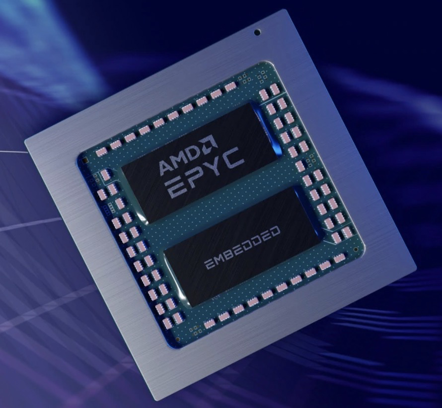
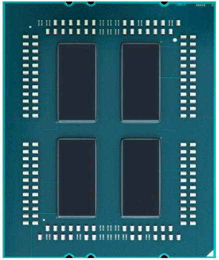
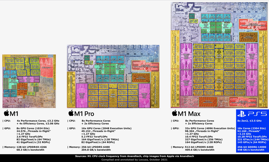
Apple M1
The M1
The critically-acclaimed M1 processor delivers:
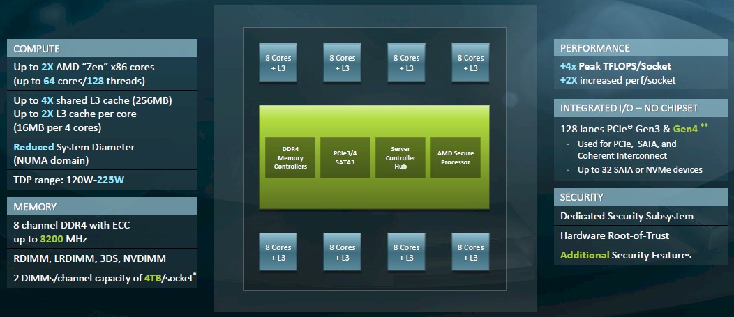
16 billion transistors and a 119mm squared-die size.